This article features a low parts count ACDC 5 Watts Charger Design with an output voltage of 5V and a maximum charge current of 1A. This is applicable for cell phones, tablets and other devices and gadgets that use 5 volt supply. This is a constant voltage constant current charger. A constant voltage means a steady level of the output voltage once full charge state has been reached. A constant current means a maximum charge current is controlled despite the battery is very drain and want to draw a high current in the few minutes’ right after it is connected to the charger. In this case, both the battery and the charger itself are protected from over current damage. This design uses an offline Flyback converter with primary side regulation. With primary side regulation, there is no need for Optocoupler and associated circuits thus lesser parts count.
Download the schematic in PDF here.
Controller Features
The controller used in this design is UCC28700 with the following features:
- Less than 30 milliwatts no load power consumption for 5-star rating
- It operates on primary side regulation thus no need Optocoupler and associated circuits
- with high voltage and current regulation accuracy
- Can support up to 130 kHz frequency thus able to use a smaller transformer
- Operates in quasi resonance so high efficiency is attainable
- Improve EMI compliance due to frequency-jitter scheme (patent pending)
- Can support wide VDD range thus a smaller bias capacitor is possible
- Clamped gate drive voltage for MOSFET
- Over voltage protection, low line and over current
- Programmable cable compensation
- SOT-23 package
ACDC 5 Watts Charger Design Specifications
Input voltage: 100Vac to 240Vac
Input Frequency: 50/60 Hz
Constant Output Voltage: 5V
Output Ripple Voltage: Less than 50mV
Constant Current: 1A
Design Applications
- Adapters and chargers with USB compliant for consumer electronics
- Cell phones, tablets, cameras and the likes
- AC-DC power supply
Design Notes
– R1 controls the in-rush current so that the bridge will not damage once C1 is fully empty than the charger is plug to AC outlet.
– BR1 is the bride rectifier that converts AC-DC. It can be replaced with four diodes using 1N4007 if economical than the existing part
– C1 serves as the DC link capacitor. The larger the better to achieve a good DC level. But a larger capacitance results to a physically bigger capacitor.
– D4, C3, R13 and R15 are parts of the RCD clamp network. They will clamp the voltage so that the MOSFET Q1 will not damage. In actual testing, if the drain voltage of Q1 is not exceeding the rating, the RCD clamp parts are can be removed to save space.
– R6, R7 and R8 are boot strap resistors needed to power the controller. Once the controller start giving pulse, the transformer auxiliary winding on pin 4 will be the one to supply the controller.
– R10 and R11 set the constant voltage while R4 and R5 set the constant current
– D1 is the secondary rectifier diode
– C4 is the output bulk capacitor. Increase the capacitance if the target ripple is not meet.
– A fuse is can be installed before R1, but for low power design, the IC protection is enough
– For more information, consult the UCC28700 datasheet and application note
Parts List
Below parts list is based on the smallest form factor possible. In case you have much space, you can increase the value of C1 and C4.
Download the parts list in excel here.
Simulation Results
Below simulation result indicates how good the constant current and constant voltage features of this AC-DC 5 Watts Charger. At any load below 1A and until 1A, the charger output is within regulation of 5V (constant voltage). When the load is increased slightly above 1A, the voltage output starts to decrease and the current is being maintained (constant current) until the output turn off (protection level triggered) when the load is further increasing.
Output Ripple Voltage
Output Capacitor Ripple Current
MOSFET Q1 Current
MOSFET Q1 Drain Voltage
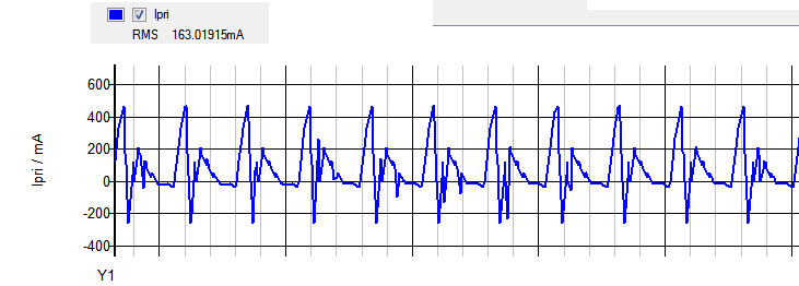
Input Current at 240Vac
Input Current at 100Vac
If you tried this, please provide feedback whether working or not. If it works directly without any tuning, its very good and we can share this to everybody. If there are issues, please feedback so that we can solve until this will become a full working design.


