
Basic NPN Transistor Principles
Universities are covering this topic very well but despite I still attempt to discuss NPN transistor principles that I think easier to understand for non technical people. NPN transistor is the name given to a bipolar junction transistor with two N type materials or negative carriers while there is only one P type material or positive carrier. NPN transistors are using below schematic symbols.

NPN transistors are using below structure to define its material composition. There are two N type materials sandwiching the P type material. In the N type material, negative charge is dominant while positive charge is dominant in the P type material.

NPN transistor is can be viewed as two diodes with connected anodes as below figure. For a diode, anode is basically the positive terminal while cathode is the negative terminal and NPN transistor has two diodes with connected anodes as the P type material is sandwich by two N type materials.

NPN transistor nowadays comes in variety of packages. For instance the popular small power, NPN transistor BC817 by nexperia has several packages as SOT23, SOT323 and SOT54.
On the other hand, power packages for NPN transistor are TO-220-3, TO-252-3 (DPAK), TO-204-2 (TO-3) and SOT-223.
NPN transistors are useful in logic implementations, electronic switches, relay drivers, motor drivers and amplifier applications.
NPN Transistor Principles and Electrical Property
Bipolar junction transistor in general is a current controlled device. What this means? This means, it needed a current flow to its base for it to function normally as expected. It is not the level of the voltage applied to the base but the amount of current flowing to the base that makes the transistor to operate. With this property, it is now obvious that you need a resistor in series with the base to set the level of current flowing through the base.
Actually, there are only two general things to remember in dealing with NPN transistor principles:
1. Turn on the device
2. Set the operation mode
At first, you need to turn on the transistor before the current can flow to the base. To turn on a transistor, the base-emitter junction must overcome. The voltage needed to overcome the base-emitter junction (VBE in short) is same with a diode drop; around 0.7V.

In actual application, VBE must be based on the datasheet of the transistor used. For instance BC817-25 of nexperia, VBEsat varies with temperature and collector current. See below graph.
nexperia has some great offerings for NPN transistor. Visit them at https://www.nexperia.com/ to check full product offerings.

(Some datasheet uses VBEsat to define base-emitter voltage).
In usual applications the applied voltage to the base is always much higher than the VBEsat, thus the VBEsat variation may not a problem. However, the variation on the VBE if not properly considered will jeopardize the transistor operation as the base current will change and then there will be change on the collector current as well, when operating in the active region.
Once VBE is overcome, being a current controlled device will take place. The amount of collector current will strongly depends on the level of the base current as long as the operation is in active region.
The base and collector current of NPN transistor is related by the term beta (β).
Beta = IC / IB
Once the NPN transistor is ON, you can set its operation mode whether amplifier or switch. These rely on the amount of base current.
Some terminologies used in Transistors
1. Beta or HFE – Beta and HFE are used interchangeably by manufacturers. Do not be confused as both of them refer to the current gain of a transistor particularly the ratio IC to IB.
Beta = HFE = IC / IB
2. Current gain – the ratio of two currents
3. Base current (IB) – current flowing through the base
4. Collector current (IC) – current flowing through the collector
5. Emitter current (IE) – current flowing through the emitter
6. VBE – base-emitter voltage
7. VCE – collector – emitter voltage
8. VBC – base-collector voltage
9. VEB – emitter-base voltage
10. VCB – collector-base voltage
11. VB – Base voltage with respect to ground
12. VE – emitter voltage with respect to ground
13. VC – collector voltage with respect to ground

Some NPN Transistor Principles and Technicalities:
1. VBE – Base voltage with respect to ground minus emitter voltage with respect to ground (VB – VE)
2. VBE – Base voltage with respect to ground minus emitter voltage with respect to ground (VB – VE)
3. VCE – Collector voltage with respect to ground minus emitter voltage with respect to ground (VC – VE)
4. VBC – Base voltage with respect to ground minus collector voltage with respect to ground (VB –VC)
5. VEB – Emitter voltage with respect to ground minus base voltage with respect to ground (VE – VB)
6. VEC – Emitter voltage with respect to ground minus collector voltage with respect to ground (VE – VC)
7. VCB – Collector voltage with respect to ground minus base voltage with respect to ground (VC – VB)
For bipolar junction transistor (BJT), the largest current is the emitter current (IE), it followed by the collector current (IC) then the base current (IB). IE is simply the sum of IC and IB.
IE = IC + IB
In active operation, IB is in micro ampere range and it can be agreed that IE is approximately equal to IC.
IE ~ IC
BJT is known to its amplification property which defined by the term beta (β). Beta is mathematically defined as
β = IC / IB
So, when you encountered the term or symbol beta in datasheet, this means the ratio of the collector current to the base current.
NPN transistor is can be operated in three regions:
1. Active
2. Cut-off
3. Saturation
The shaded in gray of below illustration is the active region. In light blue shade is the cut-off region while saturation region in orange shade. In the active region, NPN transistor operation is defined in terms of the DC load line. This is the line that can be traced when the NPN operation moves due to variation in base current (IB1 to IB6), VCE and IC. The Q point on the figure simply tells where on the DC load line the NPN operation falls.
In active region, an increase in the base current will have a corresponding increase in the collector current, as describe in below equation.
IC = β X IB

In the saturation region, IC or collector current is at maximum. In this region, any increase of the base current will have no more effect on the collector current. Thus, the equation
IC = β X IB
is not anymore valid this time.
In the cut-off region on the other hand, there is no collector current as well as zero base current. At this region, the NPN transistor is simply at off state. In this region, the VCE is equal to the collector supply.
NPN Transistor Connection Requirements
1. Collector supply (VCC) – Must not exceed allowable VCE voltage (positive voltage)
(The allowable VCE voltage is provided in the transistor datasheet and mostly described as VCEo or open base collector-emitter voltage)
2. Base bias voltage – must be larger than VBE requirements (positive voltage)
3. Base resistor – this will set the base current
4. Emitter resistor – set emitter voltage and current
5. Collector resistor – set collector voltage and current
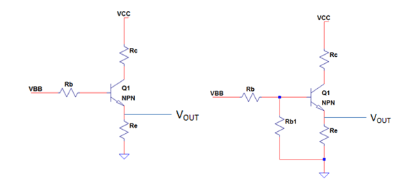
Below are some common connections for NPN transistors:


Variation 1 is the simplest connection. It has VCC which is the collector supply and VBB which is the applied voltage to the base. It has base and collector resistance; Rb and Rc. This connection is very common for low side driving.
Variation 2 has emitter resistor added. This resistor sets the emitter voltage. This is common for active operation. Variation 3 is the same to Variation 1 except there is added resistor Rb1. Rb1 ensures the base will automatically connects to ground once the applied voltage VBB do not have a low state. In this reason, noise is prevented to falsely turn on the NPN transistor.
Variation 4 is the same to variation 3 plus a resistor Re in the emitter. The added resistor sets the emitter voltage. It is easy to set the operation of the NPN transistor into active region with the addition of Re.
Variation 5 is actually the same to Variation 4. The only difference is that VBB is taken from the VCC. Variation 6 is also the same to variation 4 and 5. Do not be confused of the capacitors C1 and C2. At DC analysis, these capacitors are treated open and thus not part of the circuit at all reducing the circuit to that of variation 4 and 5.
Variation 7 is the same to Variation 3 only that VBB is taken from VCC. Variation 8 is the same to variation 3 and 7. The added capacitors C1 and C2 are not part of the circuit at DC analysis.
Variation 4, 5 and 6 are called voltage divider bias. Voltage divider bias is the most stable type of connecting NPN transistor. The bias is stable to variations in device beta. In some applications, it is also minimizing the effect of VBE variations.
Factors that Affect Stability
NPN transistor principles should not only limited to setting right bias, it is also needed to identify some factors that will affect stability. Stability is very important in mass production and long term operation. The common factor that affect NPN transistor stability is operating temperature, VBE variation and Beta variation. Operating temperature can affect NPN transistor parameters. In designing a circuit, it is a must to consider the effect of operating temperatures. The VBE may vary from device to device. It will also vary with the operating temperature. Beta will vary from device to device even in a same lot. Beta usually has wider range. Be careful to consider the variation in designing a circuit.
Voltage divider bias (VDB) will minimize the variations mentioned above. VDB is actually the most stable type of biasing.
How Voltage Divider Bias Minimizes NPN Transistor Circuit Variations and Improved Noise Immunity
Variations 4, 5 and 6 are all VDB. Let us simplify further why so VDB is called the most stable type of bias or connection diagram.
Consider the given values below:
VCC = 10V, Rb = 135kΩ, Rc = 1kΩ, Rb1 = 10kΩ, Re = 24Ω, β = 353, VBE = 0.62
With below circuit (VDB), the computed values are:


When the beta drifts to 200, the new values are:

As you can see, there is only around 0.4V increase in the level of VOUT despite large decrease in beta.
Let us compare the result to a non-voltage divider bias. Let us simply remove the emitter resistor as below circuit.

For a beta of 353, the computed values are:

When beta became 200, the computed results are:

As you noticed, there is around 1.2V increase on the VOUT. This is huge compared to the voltage divider bias that is only around 0.4V.
The next question to answer is how a voltage divider bias improves noise immunity?
Let us consider a voltage divider bias in below circuit. In actual applications, VBB is can be a standalone source coming from a logic circuit or a microcontroller and the likes. There is a tendency that VBB does not have a defined low logic. If there is no presence of Rb1, the transistor base will be floating by the time you intend to turn off the transistor. This is not a good design practice as noise can trigger the base and falsely turn on the transistor.

With the presence of RB1, there is no chance that noise can falsely turn on the base as the base is tied to circuit ground through RB1.
How to determine if a Transistor is NPN?
1. Using Internet – if you know the part number, then it is very easy to determine if you have internet connections.
2. Using a digital meter – if you have a digital meter, set it to diode mode. Put the meter probe to any two pins. Once you get a diode drop (0.5V~0.7V), you either measured the base-emitter or base-collector. Put one probe steady to one pin while the other probe to any of the two other pins, one at a time. Once you read the same diode drop, you get the transistor base pin on the steady probe. If the steady probe is positive, the transistor is NPN. If the steady probe is negative, then the transistor is PNP.
NPN Transistor General Uses
There are varieties of applications where NPN transistors are used. Let us consider the most common; 1. Switch 2. Logic and 3. Amplifier
For switch and logic applications, the transistor is set to operate at cut-off and saturation.

For amplifier, the transistor operation is confined in the active region only.

Switch and Logic Operation
In order to operate the transistor to these functions, it must be driven into saturation and cut-off. To saturate, there should be enough base current. To cut-off, there should be a way to turn off the transistor.
How to Saturate NPN Transistor
1. First thing to do is to select the right circuit configuration
Select the circuit structure that has little dependence to the device beta. To guide you, select variation 1 and 3.

Personally, I will choose variation 3 due to the presence of Rb1 that will add noise immunity
2. Define current set point for either the base or collector
3. Set the collector current (IC) to base current (IB) ratio to 2 (or lower)
4. Compute the Resistances
5. Double check the circuit using the selected values
Example 1
In applications that the VBB is provided by a microcontroller unit (MCU) or any small power circuit, it is a good practice to consider the base current set point such that it will not exceed the microcontroller or small power circuit rating. For example, the maximum source current that can be provided by MCU is 4mA, set the base current (IB) to at most 75% of this; so, a set point current of 3mA for the base.
1. Select circuit configuration: Considering Variation 1 with VBB = 5V, VCC = 10V

2. Set base current IB
IB = 3mA
3. Set the collector current (IC) to base current (IB) ratio to 2 (or lower)
The ratio of 2 is very hard saturation already. Some datasheets considers 10 as hard saturation.
IC / IB = 2
IC = 2 X IB = 2 X 3mA = 6mA
4. Compute Resistances
a. Solve Rb
The value of Rb is easy to solve using below formula:
Rb = (VBB-VBE) / IB
You can assume VBE of 0.7V and this gives 1433.33 ohms for Rb. The closest standard resistor value is 1.43k, so use this value.
(Here, we used VBE of 0.7V despite the fact that VBE may vary up to 1.2V at worst case scenario as explained earlier. However, since we set the ratio of IC to IB to 2, this ensures a hard saturation and VBE variation don’t have effect on this anymore.)
b. Solve Rc
Rc is can be solved using the formula below:
Rc = VCC / IC = 10V / 6mA = 1.67kΩ
The closest standard value is 1.69kΩ; use this value.
5. Double check the circuit using the selected values
Here, I did simple simulations with the selected values. I used here BC817-25 transistor. The simulation shows a base current I(Rb) of 3mA while 6mA for collector current I(Rc). The red line is VOUT which is taken on the transistor collector. It reads 0V that means the transistor is saturating.


Example 2
1. Select circuit configuration: Considering Variation 3 with VBB = 5V, VCC = 10V

2. Set base current IB
IB = 3mA
3. Set the collector current (IC) to base current (IB) ratio to 2 (or lower)
IC / IB = 2
IC = 2 X IB = 2 X 3mA = 6mA
4. Compute Resistances
a. Set IB1
When using variation 3, you can simply budget IB1 current 1% of IB. This means that the Rb1 value is relatively high compared to Rb and this is practical because Rb1’s is intended to be high resistance.
IB1 = 0.01 X 3mA = 30µA
b. Solve Rb1
Then Rb1 is can be solved using below equation:
Rb1 = VBE / IB1 = 0.7V / 30µA = 23.33kΩ
The closest standard value is 23.4kΩ; use this value.
c. Solve Iin
Iin is just the sum of IB and IB1. So
Iin = IB + IB1 = 3mA + 30µA = 3.03mA
d. Solve Rb
To solve Rb, use below formula
Rb = (VBB – VBE) / Iin = (5V – 0.7V) / 3.03mA = 1.419kΩ
The closest standard value is 1.43kΩ; use this value.
e. Compute Rc
Rc is can be solved using the formula below:
Rc = VCC / IC = 10V / 6mA = 1.67kΩ
The closest standard value is 1.69kΩ; use this value
5. Double check the circuit using the selected values
Here, I did simple simulations with the selected values. I used here BC817-25 transistor. The simulation shows a base current Ib(Q1) of 3mA while 6mA for collector current Ic(Q1). The dark blue line is VOUT which is taken on the transistor collector. It reads 0V that means the transistor is saturating.


For more discussions on how to saturate NPN transistor, kindly read the articles Transistor Operation Mode Determination, How to know if a Transistor is Saturated? and How to Drive a Transistor into Hard Saturation.
Derived Equations for Common NPN Transistor Circuits
Here are common NPN transistor circuits with derived equations.
Variation 1

Variation 2

Variation 3

Variation 4

Amplifier Configurations
Common Emitter Configuration
All circuits below are common emitter. Common emitter simply means that the emitter is not connected directly to either input or output. In below circuits, VBB is the input and it is connected to the base while output is taken at the collector. Common emitter is the most popular amplifier configuration.

Common Collector Configuration
Below circuits are common collectors. Common collector simply means that the collector is not directly connected to either input or output. VBB is the input which is applied to the base while the output is taken at the emitter. Common collector is also called as emitter follower.
Common Base Configuration
Below is a common base configuration. This configuration is not popularly used. I myself have not used this in actual applications.

NPN Transistor as a Relay Driver
NPN transistor is easy to be configured as relay driver. As a relay driver, NPN acts as a low side switch. This means that the NPN itself will be the one providing ground path to the other side of the relay. Below is a relay driver circuit. The relay is composed of Lcoil and Rcoil which mean coil inductance and coil resistance respectively.

Q1 will be the one to connect the low side of the relay to ground for the coil to energize. When there is high signal at VIN node, Q1 will saturate and connect the relay to ground. On the other hand, when there is no signal at VIN node, Q1 will cut-off the path of the relay. R2 in this application will add noise immunity especially when the source at VIN node is either positive voltage or open. D1 is use to protect the transistor for the relay back EMF of kickback voltage. D1 is very important, do not forget it!
Proper Component Selection
A relay driver should connect the other side of the relay to the ground (or positive supply for other implementations) with ideally zero voltage drop. This means that the transistor should operate in hard saturation. Hard saturation simply means that even in worst case scenario, the transistor will remain in saturation.
Example:
Let us supply the right values to the above circuit. V1 = 12V, VIN = 5V, Rcoil = 330Ω.
1. Solve collector current (IC)
IC = V1 / Rcoil = 12V / 330Ω = 36.37mA
2. Set base current to guarantee hard saturation
An value of IC/IB from 10 and below is considered hard saturation. Let us consider here 10 in this example. However, you still need to check the minimum beta of the transistor use in application. The selected IC/IB must be very much lower than the minimum beta specified in the datasheet.
IC/IB = 10
IB = IC / 10 = 36.37mA / 10 = 3.64mA
You cannot just simply set the IC/IB ratio to very low value because this will give high base current. You must set base current value that will not exceed the current capability of the circuit providing the signal at the VIN node.
3. Compute the resistances
For a VIN = 5V, R2 is can be set to 10kΩ. R2’s purpose is only to ensure the base will connect to ground when VIN has open state, thus 10kΩ is a good value already.
Since R2 is known, the current flowing through it is can be solved as
IR2 = VBE / R2 = 0.7V / 10kΩ = 70uA
We used here 0.7V for VBE as transistors VBE typical value is 0.7V. For exact calculation, you may consider the datasheet of the part you are using.
Then, the current on R3 is can be calculated as well using:
IR3 = IR2 + IB = 70uA + 3.64mA = 3.71mA
Finally, R3 is can be computed using below equation:
R3 = (VIN – VBE) / IR3 = (5V – 0.7V) / 3.71mA = 1.16kΩ.
Select the closest resistor standard value.
4. Calculate power dissipation
After all values are known, we will proceed to power calculation. Selecting under rated devices will lead to circuit failure.
A. Q1 Power Dissipation
PQ1 = IB X VBE + VCE X IC
In above calculation, we are not considering the actual device VCEsat (or saturation level of the VCE). This is not zero in actual even though how much saturated the transistor is. Always consult the datasheet. Let us use 100mV in this example. So,
PQ1 = IB X VBE + VCE X IC = 3.64mA X 0.7V + 0.1V X 36.37mA = 6.185mW
B. R2 Power Dissipation
PR2 = IR2 X IR2 X R2 = 70uA X 70uA X 10kΩ = 49uW
C. R3 Power Dissipation
PR3 = IR3 X IR3 X R3 = 3.71mA X 3.71mA X 1.16kΩ = 16mW
D. Relay Power Dissipation
PRelay = IC X IC X Rcoil = 36.37mA X 36.37mA X 330Ω = 436.5mW
Select parts that have higher power rating compared to the calculation result above.
I did simple simulations to verify the circuit using the selected values. I get a VCE of around zero volt that means the transistor is saturating. I get also a collector current of 36mA which is the same to the computed value.


How to Troubleshoot NPN Transistor Circuits
General
In troubleshooting, it is essential to know the basic facts about NPN transistor. You need to know that VBE may range from 0.6V-1.2V (though 1.2V is under worst case scenario). When you put the positive voltmeter probe on the base while the negative probe to the emitter, you must read within 0.6V-1.2V, once the circuit is powered up. If you read 0V, the transistor base-emitter is shorted. On the other hand if you read a level same to VBB or applied voltage to the base, the transistor base-emitter is off or simply the transistor is not conducting.
If the transistor circuit is set to operate at saturation, you must read 0V across VBE by putting the positive voltmeter probe to the collector while negative probe to the emitter, once the circuit is powered up and there is a positive supply to the base. On the other way around, if there is no supply to the base or the base voltage is negative, you should read a level the same to VCC.
Specific Circuits
A.

Failure mode: Output always low (0V)
Possible defects:
- Shorted Q1
- Open Rc
Failure mode: Output always high
Possible defects:
- Open Rb
- Defective Q1
Failure mode: Output is intermittent low and high
Possible defects:
- Bad solder on Rb or defective Rb
- Bad solder on Q1 or defective Q1
- Bad solder on Rc or defective Rc
B.


Failure mode: Output always low (0V)
Possible defects:
- Shorted Re
- shorted both Re and Q1
Failure mode: Output always VCC
Possible defects:
- open Q1
- open Re
- shorted Rc
Failure mode: Output is not zero, not VCC, not intermittent but not correct based on calculation
Possible defects:
- Open Rc
Failure mode: Output is intermittent
Possible defects:
- Check all parts for bad solder
- if no cold solder, there is a partially defective part. Measure the resistances and conduct diode test to Q1.
C.

Failure mode: Output always low (0V)
Possible defects:
- Open Rc
- Shorted Q1 C-E
Failure mode: Output always high or VCC
Possible defects:
- defective Q1
- open Rb
- shorted Rb1 (or changed to a lower value)
Failure mode: Output is intermittent
Possible defects:
- Check all parts for bad solder
- if no cold solder, there is a partially defective part. Measure the resistances and conduct diode test to Q1.
Great tutorial, could you please spare a moment and have a look at this circuit. Q1 is normally on and Q2 is biased off and it must stay off. When reed sensor opens, Q1 turns off and a short pulse from C1 through Q2 turn the SCR on. My question is there a better way to reliably bias Q1 on and Q2 off to avoid false trigger? Also what do you think about sensor wire input protection C2,C4 and C5? please note R1 and R3 must be high value to minimise the current consumption.
https://www.imageupload.co.uk/image/BuHL
Ib of variation 4 seems not understandable. Could you please explain why the denominator has the portion of Rb and Rb1 connected in parallel value?